SI2306(N)
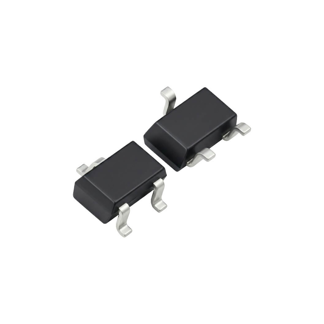
The image is for illustrative purposes only; please refer to the product data sheet for precise specifications.
GET QUOTE NOW!
| Part Number | SI2306(N) |
|---|---|
| Manufacturer |

|
| Description | The SI2306(N) from GOODWORK is an N-Channel Enhancement Mode MOSFET designed for compact power switching, load control, DC-DC conversion, and general-purpose power management applications. The device combines a 30V drain-source voltage rating, continuous drain current capability of up to 3.16A, and low on-state resistance in a compact SOT-23 surface-mount package. The SI2306 features a maximum drain-source voltage (VDS) of 30V and supports continuous drain current up to 3.16A under the manufacturers specified conditions. Maximum power dissipation is approximately 0.75W, making the device suitable for low- and medium-power switching circuits where PCB space is limited. Low conduction loss is achieved through its low RDS(on). The GOODWORK datasheet specifies a typical drain-source on-resistance of approximately 38mΩ at VGS = 10V and ID = 3.5A, with a maximum value of 47mΩ. At VGS = 4.5V and ID = 2.8A, RDS(on) is typically 52mΩ and specified at a maximum of 65mΩ. These characteristics help reduce conduction losses and improve power efficiency in switching applications. The gate threshold voltage is specified between 1.0V and 3.0V at a drain current of 250µA. The MOSFET is characterized for operation with 4.5V and 10V gate drive levels, providing convenient interfacing with many power-management and gate-drive circuits. The SI2306 also provides low gate-charge characteristics for efficient high-speed switching. Typical gate charge is approximately 3nC at VGS = 5V, while total gate charge is approximately 6nC at VGS = 10V. Low gate charge reduces the energy required to switch the MOSFET and helps minimize gate-driver losses in PWM and DC-DC converter applications. Typical input capacitance is approximately 305pF, output capacitance is approximately 65pF, and reverse transfer capacitance is approximately 29pF. The device also offers fast switching characteristics, with typical turn-on delay, rise, turn-off delay, and fall times of approximately 7ns, 12ns, 14ns, and 6ns, respectively, under the manufacturers specified test conditions. The integrated body diode provides a typical forward voltage of approximately 0.8V at 1.25A, with a specified maximum of 1.2V. The device supports a maximum gate-to-source voltage of ±20V, providing suitable gate-voltage tolerance for a wide variety of switching circuits. The SI2306 is specified for an operating junction temperature range of -55°C to +150°C. Its compact SOT-23 (TO-236-3) surface-mount package provides a space-efficient solution for high-density PCB layouts and automated SMT production. The SI2306(N) is widely used in DC-DC converters, load switching circuits, battery-powered equipment, power management circuits, LED drivers, motor control circuits, portable electronics, embedded systems, power supply switching stages, industrial electronics, consumer devices, protection circuits, and general-purpose high-speed switching applications requiring a compact 30V N-channel MOSFET with low on-resistance and low gate charge. |
| Product Group | Transistor |
| MOQ | 3000 pcs |
| SPQ | 3000 pcs |
| Figure/Case | SOT-23 |
| Package | T&R Pack |
 PDF Datasheet PDF Datasheet | |
| Ship From | Hong Kong |
| Shipment Way | DHL / Fedex / TNT / UPS / Others |
| Delivery Term | Ex-Works |
| Send RFQ | sales@signalhk.com |
Request quotation for
SI2306(N)
SI2306(N)