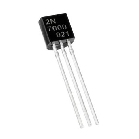
2N7000
| Part Number | 2N7000 |
|---|---|
| Manufacturer |
 ON Semiconductor ON Semiconductor
|
| Description | The 2N7000 is an N-channel enhancement-mode MOSFET designed primarily for low-power switching applications. It features a maximum drain-source voltage (VDS) of 60V, allowing it to handle moderate voltage levels. The continuous drain current (ID) is rated at 200 mA, with pulsed currents permissible up to 500 mA, making it suitable for small-load switching. It has a relatively low on-resistance (RDS(on)), typically 1.2 ohms at a gate voltage (VGS) of 10V, contributing to efficient operation with minimal power loss. The gate threshold voltage (VGS(th)) ranges from 0.8V to 3V, meaning it can be turned on with standard logic-level signals. Additionally, the input capacitance is low, around 20–50 pF, enabling fast switching speeds with minimal gate drive requirements. These features make the 2N7000 an ideal choice for digital switching, signal interfacing, and small load driving in both hobbyist and commercial circuits. |
| Product Group | Transistor |
| MOQ | 10000 pcs |
| SPQ | 10000 pcs |
| Figure/Case | TO92-3 |
| Package | T&R Pack |
 PDF Datasheet PDF Datasheet | |
| Ship From | Hong Kong |
| Shipment Way | DHL / Fedex / TNT / UPS / Others |
| Delivery Term | Ex-Works |
| Send RFQ | sales@signalhk.com |
| Parameter | Symbol | Test Conditions | Min | Typ | Max | Units |
|---|---|---|---|---|---|---|
| Drain-Source Breakdown Voltage | VDS | ID = 1 mA, VGS = 0 V | 60 | — | — | V |
| Gate Threshold Voltage | VGS(th) | VDS = VGS, ID = 1 mA | 0.8 | 2.1 | 3.0 | V |
| Zero Gate Voltage Drain Current | IDSS | VDS = 60 V, VGS = 0 V | — | — | 1 | µA |
| Gate-Body Leakage Current | IGSS | VGS = ±20 V | — | — | ±100 | nA |
| Drain On-State Resistance | RDS(on) | VGS = 10 V, ID = 500 mA | — | — | 5 | ? |
| Forward Transconductance | gFS | VDS = 10 V, ID = 500 mA | 0.1 | — | — | S |
| Input Capacitance | Ciss | VDS = 25 V, VGS = 0 V, f = 1 MHz | — | 50 | — | pF |
| Output Capacitance | Coss | Same as above | — | 20 | — | pF |
| Reverse Transfer Capacitance | Crss | Same as above | — | 10 | — | pF |
| Turn-On Delay Time | td(on) | VDD = 15 V, RL = 25 ?, VGS = 10 V | — | — | 10 | ns |
| Rise Time | tr | Same as above | — | — | 20 | ns |
| Turn-Off Delay Time | td(off) | Same as above | — | — | 10 | ns |
| Fall Time | tf | Same as above | — | — | 20 | ns |
| Total Gate Charge | Qg | VDS = 25 V, ID = 500 mA | — | — | 2.0 | nC |
| Drain-Source Diode Forward Voltage | VSD | IS = 500 mA, VGS = 0 V | — | — | 1.5 | V |
| Continuous Drain Current | ID | TA = 25°C | — | — | 200 | mA |
| Pulsed Drain Current | IDM | Pulse width ? 10 µs | — | — | 500 | mA |
| Total Power Dissipation | PD | TA = 25°C | — | — | 400 | mW |
| Thermal Resistance, Junction to Ambient | R?JA | — | — | — | 312.5 | °C/W |
| Operating Junction Temperature Range | TJ | — | -55 | — | +150 | °C |
| Storage Temperature Range | Tstg | — | -55 | — | +150 | °C |
2N7000
