FDS89161
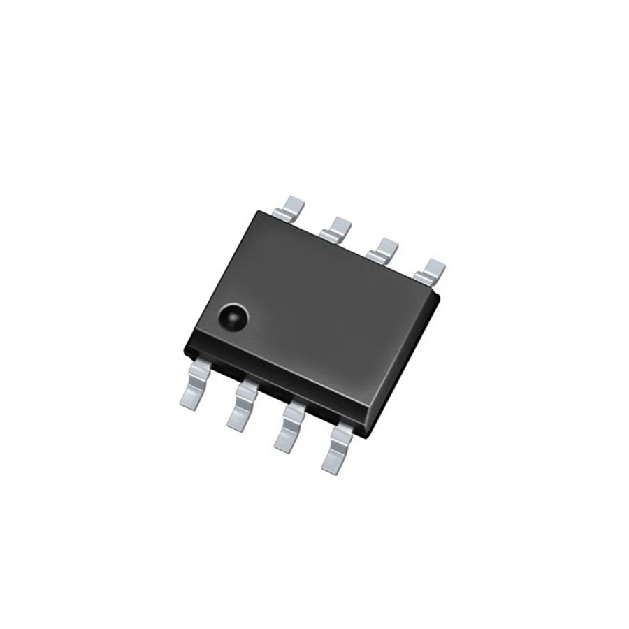
The image is for illustrative purposes only; please refer to the product data sheet for precise specifications.
GET QUOTE NOW!
| Part Number | FDS89161 |
|---|---|
| Manufacturer |
 ON Semiconductor ON Semiconductor
|
| Description | The FDS89161 is a dual N-channel power MOSFET from onsemi, originally developed using Fairchild Semiconductor's advanced PowerTrench® Shielded Gate technology. The device integrates two independent N-channel MOSFETs into a single compact SOIC-8 package and is optimized for low on-resistance, fast switching performance, and high ruggedness. Each MOSFET provides a maximum drain-to-source voltage (VDSS) of 100V, making the FDS89161 suitable for medium-voltage switching power supplies, synchronous rectification stages, bridge converters, and other power conversion applications requiring substantial voltage capability in a compact surface-mount package. The device supports a maximum continuous drain current (ID) of 2.7A at specified conditions. The maximum pulsed drain current capability is approximately 15A, allowing the MOSFETs to tolerate short-duration current peaks within the limits defined by the device safe operating area and thermal characteristics. The FDS89161 provides a maximum RDS(on) of 105mΩ at VGS = 10V and ID = 2.7A. Low drain-to-source resistance reduces conduction losses and improves efficiency in switching power conversion applications. At a lower gate drive voltage of VGS = 6V, the maximum RDS(on) is approximately 171mΩ at ID = 2.1A. These characteristics allow the device to be used with a variety of gate-drive circuits while maintaining predictable conduction performance. The FDS89161 is manufactured using Shielded Gate PowerTrench® MOSFET technology. This process is optimized to provide a combination of low RDS(on), low gate charge, efficient switching characteristics, and device ruggedness, making it suitable for high-frequency power conversion designs. The maximum gate-to-source voltage (VGS) is ±20V. Designers should ensure that gate-drive voltages and switching transients remain within this rating to maintain reliable long-term operation. The device features a maximum total gate charge (Qg) of approximately 4.1nC at VGS = 10V. The relatively low gate charge reduces the energy required to switch the MOSFET and helps minimize gate-driver losses in high-frequency switching applications. The maximum input capacitance Ciss is approximately 210pF at VDS = 50V. Low capacitance and optimized switching characteristics help the device achieve efficient operation in compact switching power supplies and converter stages. The FDS89161 has a maximum gate threshold voltage VGS(th) of 4V at ID = 250µA. Gate threshold voltage indicates the beginning of MOSFET conduction and should not be interpreted as the recommended gate voltage for achieving the specified low RDS(on) values. Both N-channel MOSFETs are electrically independent within the package, allowing designers to configure them for a variety of switching topologies. The dual-device construction can reduce PCB area and simplify layout compared with using two separate discrete MOSFET packages. The device is particularly suitable for synchronous rectification, where low conduction resistance and fast switching help improve power conversion efficiency. It can also be used as a primary switching device in bridge converter topologies and other high-frequency switching circuits. The FDS89161 is 100% UIL tested, providing additional assurance of MOSFET ruggedness under unclamped inductive switching conditions. The device has a specified single-pulse avalanche energy rating of approximately 13mJ under the conditions defined by the manufacturer. The maximum junction temperature is +150°C, with an operating and storage junction temperature range of approximately -55°C to +150°C. Appropriate PCB copper area, thermal design, switching frequency, and current derating should be considered to maintain junction temperature within the specified limits. The FDS89161 is supplied in an industry-standard 8-lead SOIC package with an approximately 3.90mm body width. The widely used surface-mount package provides a practical combination of compact dimensions, manufacturability, electrical performance, and thermal capability. The device is supplied in tape-and-reel packaging with 2500 pieces per reel, making it suitable for automated SMT assembly and high-volume electronics manufacturing. The FDS89161 is also Pb-free, halide-free, and RoHS compliant. The combination of dual N-channel configuration, 100V drain-to-source rating, 2.7A continuous drain current, 105mΩ maximum RDS(on), low gate charge, Shielded Gate PowerTrench technology, and compact SOIC-8 packaging makes the FDS89161 an efficient solution for medium-voltage switching applications. The FDS89161 is widely used in synchronous rectifiers, bridge converters, primary-side power switches, DC/DC converters, AC/DC power supplies, isolated power converters, industrial power electronics, telecommunications power supplies, embedded power systems, battery-powered equipment, power management circuits, motor control electronics, and other high-efficiency switching applications. |
| Product Group | Transistor |
| MOQ | 2500 pcs |
| SPQ | 2500 pcs |
| Figure/Case | SOIC-8 |
| Package | T&R Pack |
 PDF Datasheet PDF Datasheet | |
| Ship From | Hong Kong |
| Shipment Way | DHL / Fedex / TNT / UPS / Others |
| Delivery Term | Ex-Works |
| Send RFQ | sales@signalhk.com |
Request quotation for
FDS89161
FDS89161