XC7S50-2CSGA324C
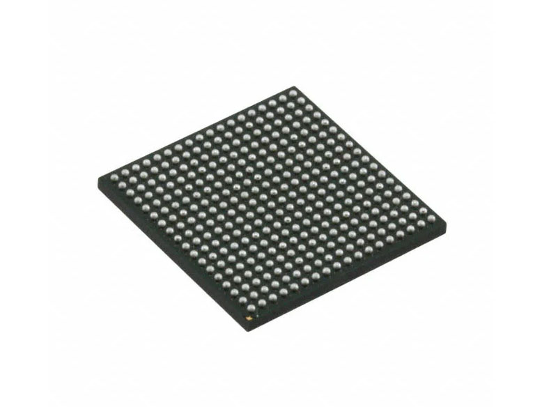
The image is for illustrative purposes only; please refer to the product data sheet for precise specifications.
GET QUOTE NOW!
| Part Number | XC7S50-2CSGA324C |
|---|---|
| Manufacturer |
 AMD Advanced Micro Devices Inc. AMD Advanced Micro Devices Inc.
|
| Description | The XC7S50-2CSGA324C is a high-performance Spartan-7 Field Programmable Gate Array (FPGA) from AMD Xilinx, designed to provide programmable logic, embedded memory, DSP processing, flexible I/O, and advanced clock management in a cost-optimized and power-efficient device. It is suitable for industrial control, communications, embedded processing, video, instrumentation, and high-speed digital interface applications. The XC7S50 device provides approximately 52,160 logic cells, giving designers substantial programmable logic resources for implementing custom digital architectures, state machines, communication protocols, signal-processing functions, control logic, and hardware acceleration. The programmable fabric includes approximately 32,600 6-input Look-Up Tables (LUTs) and 65,200 flip-flops. These resources can be configured through the AMD Vivado Design Suite to implement highly parallel digital systems that would otherwise require multiple discrete logic devices or dedicated ASIC circuitry. The XC7S50 integrates approximately 2,700Kb of Block RAM. Internal Block RAM resources can be configured for applications such as data buffers, FIFOs, lookup tables, processor memory, image and signal-processing buffers, communication queues, and temporary storage without requiring external memory for many embedded functions. For arithmetic and digital signal-processing applications, the XC7S50 incorporates 120 DSP48E1 slices. These dedicated DSP resources efficiently implement multiplication, accumulation, filtering, modulation, control algorithms, mathematical processing, and other computationally intensive functions while reducing consumption of general-purpose FPGA logic. The XC7S50-2CSGA324C provides up to 210 user I/O pins in the CSGA324 package. Spartan-7 High-Range SelectIO resources support numerous single-ended and differential interface standards, allowing the FPGA to connect directly to a wide variety of digital peripherals and external devices. The High-Range I/O architecture supports I/O bank voltages from approximately 1.2V to 3.3V, depending on the selected interface standard. This flexibility allows the FPGA to interface with multiple logic families and voltage domains within the same system. Spartan-7 devices incorporate advanced clock management resources including Mixed-Mode Clock Managers and Phase-Locked Loops. These resources provide clock multiplication, division, phase shifting, jitter filtering, frequency synthesis, and distribution for complex synchronous digital systems. The XC7S50 also provides extensive global and regional clock-routing resources designed to distribute clocks with low skew throughout the programmable logic fabric. This enables reliable implementation of designs containing multiple clock domains and high-performance synchronous logic. The Spartan-7 architecture is based on AMD Xilinx's established 7 Series FPGA technology and uses a 28nm process optimized for a combination of performance, power efficiency, programmable logic density, and cost. The architecture shares many development concepts and design resources with other members of the Xilinx 7 Series FPGA portfolio. The -2 designation identifies the device's speed grade. Within the standard Spartan-7 product family, the -2 speed grade provides the highest performance level compared with the standard -1 speed grade, making the XC7S50-2CSGA324C suitable for designs requiring improved timing performance. The C suffix identifies the commercial temperature grade. This device is intended for commercial-temperature applications where the FPGA junction temperature is maintained within the manufacturer's specified operating limits. The FPGA core predominantly operates from a nominal 1.0V VCCINT supply. Additional supply rails are used for auxiliary circuitry and programmable I/O banks, allowing individual I/O banks to operate with voltage levels appropriate for the selected interface standards. Spartan-7 configuration architecture supports external nonvolatile configuration memories and standard FPGA configuration methods. After power-up, the device loads its configuration bitstream to establish the required programmable logic, routing, I/O, memory, DSP, and clocking architecture. The device is supported by the AMD Vivado Design Suite, providing synthesis, implementation, timing analysis, simulation, IP integration, debugging, bitstream generation, and device programming capabilities. Designers can develop FPGA logic using HDL languages such as VHDL and Verilog as well as supported IP-based design methodologies. The XC7S50 architecture provides substantial flexibility for implementing custom communication interfaces. Programmable logic and SelectIO resources can be used for SPI, UART, I2C, parallel buses, differential interfaces, proprietary protocols, sensor interfaces, memory interfaces, and other application-specific digital communication functions. The combination of programmable logic and 120 dedicated DSP slices makes the device particularly useful for real-time digital signal processing. Applications can include FIR and IIR filters, motor-control algorithms, sensor processing, digital modulation, image processing, waveform generation, industrial control, and hardware acceleration. The XC7S50-2CSGA324C is supplied in a 324-ball CSGA chip-scale BGA package measuring approximately 15 × 15mm. The package uses a 0.8mm ball pitch and provides 324 solder balls, allowing a high number of user I/O and power connections within a relatively compact PCB footprint. The CSGA324 package uses lead-free Sn/Ag/Cu solder balls and is designed for surface-mount PCB assembly. Proper multilayer PCB stack-up, BGA escape routing, power distribution, decoupling, thermal design, and controlled-impedance routing should be considered when designing systems around the FPGA. The combination of 52,160 logic cells, 32,600 LUTs, 65,200 flip-flops, approximately 2.7Mb Block RAM, 120 DSP48E1 slices, 210 user I/Os, -2 speed grade, flexible SelectIO resources, advanced clock management, and compact 324-ball BGA packaging makes the XC7S50-2CSGA324C a powerful programmable platform for medium-density embedded and industrial digital systems. The XC7S50-2CSGA324C is widely used in industrial automation, motor control, machine vision, embedded computing, communication equipment, digital signal processing, video and image processing, instrumentation, test and measurement equipment, sensor processing, robotics, medical electronics, factory automation, protocol conversion, data acquisition, security systems, digital control equipment, and custom high-speed digital logic applications. |
| Product Group | FPGA |
| MOQ | 32 pcs |
| SPQ | 32 pcs |
| Figure/Case | 324-LFBGA |
| Package | TRAY Pack |
| Ship From | Hong Kong |
| Shipment Way | DHL / Fedex / TNT / UPS / Others |
| Delivery Term | Ex-Works |
| Send RFQ | sales@signalhk.com |
Request quotation for
XC7S50-2CSGA324C
XC7S50-2CSGA324C