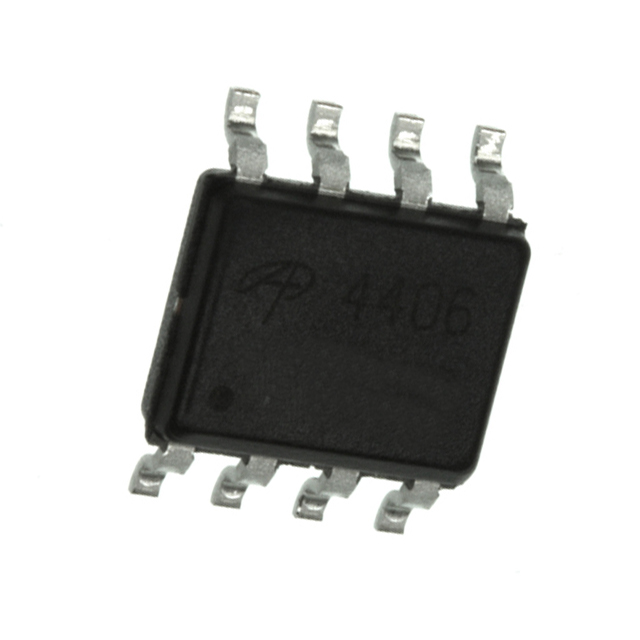
AO4480
| Part Number | AO4480 |
|---|---|
| Manufacturer |
|
| Description | The AO4480 is a dual N-channel MOSFET designed for high-efficiency power switching in compact packages. It operates with a maximum drain-source voltage (VDS) of 30V, making it suitable for low- to medium-voltage applications like DC-DC converters and load switches. Each channel can handle a continuous drain current (ID) up to 8A at a VGS of 10V, and up to 6.5A at 4.5V, providing robust current-handling for compact designs. It features a very low on-resistance (RDS(on)), typically 0.0105ohm at VGS = 10V and 0.0135ohm at VGS = 4.5V, ensuring minimal conduction losses and high efficiency. The gate threshold voltage (VGS(th)) ranges from 0.6V to 1.0V, making it fully logic-level compatible. Fast switching characteristics, low gate charge, and a compact SO-8 package make the AO4480 ideal for power management, synchronous buck converters, and battery-operated equipment. |
| Product Group | Transistor |
| MOQ | 3000 pcs |
| SPQ | 3000 pcs |
| Figure/Case | 8-SOIC |
| Package | T&R Pack |
 PDF Datasheet PDF Datasheet | |
| Ship From | Hong Kong |
| Shipment Way | DHL / Fedex / TNT / UPS / Others |
| Delivery Term | Ex-Works |
| Send RFQ | sales@signalhk.com |
| Parameter | Symbol | Test Conditions | Min | Typ | Max | Units |
|---|---|---|---|---|---|---|
| Drain-Source Breakdown Voltage | VDS | ID = 250 µA, VGS = 0 V | 40 | — | — | V |
| Gate Threshold Voltage | VGS(th) | VDS = VGS, ID = 250 µA | 1.0 | 2.0 | 3.0 | V |
| Zero Gate Voltage Drain Current | IDSS | VDS = 32 V, VGS = 0 V | — | — | 1 | µA |
| Gate-Body Leakage Current | IGSS | VGS = ±20 V, VDS = 0 V | — | — | ±100 | nA |
| Drain On-State Resistance | RDS(on) | VGS = 10 V, ID = 14 A | — | 9.0 | 11.5 | m? |
| VGS = 4.5 V, ID = 5 A | — | 12.0 | 15.5 | m? | ||
| Forward Transconductance | gFS | VDS = 5 V, ID = 14 A | 50 | — | — | S |
| Input Capacitance | Ciss | VDS = 20 V, VGS = 0 V, f = 1 MHz | — | 1600 | 1920 | pF |
| Output Capacitance | Coss | Same as above | — | — | 320 | pF |
| Reverse Transfer Capacitance | Crss | Same as above | — | — | 100 | pF |
| Total Gate Charge | Qg | VGS = 10 V, VDS = 20 V, ID = 14 A | — | — | 22 | nC |
| VGS = 4.5 V, VDS = 20 V, ID = 14 A | — | — | 10.5 | nC | ||
| Gate-Source Charge | Qgs | Same as above | — | — | 4.2 | nC |
| Gate-Drain Charge | Qgd | Same as above | — | — | 4.8 | nC |
| Turn-On Delay Time | td(on) | VGS = 10 V, VDS = 20 V, RGEN = 3 ?, RL = 1.5 ? | — | — | 3.5 | ns |
| Rise Time | tr | Same as above | — | — | 6.0 | ns |
| Turn-Off Delay Time | td(off) | Same as above | — | — | 13.2 | ns |
| Fall Time | tf | Same as above | — | — | 3.5 | ns |
| Body Diode Forward Voltage | VSD | IS = 1 A, VGS = 0 V | 0.7 | — | 1.0 | V |
| Maximum Continuous Drain Current | ID | TA = 25°C | — | — | 14 | A |
| TA = 70°C | — | — | 11 | A | ||
| Maximum Pulsed Drain Current | IDM | Pulse width ? 10 µs | — | — | 70 | A |
| Maximum Power Dissipation | PD | TA = 25°C | — | — | 3.1 | W |
| TA = 70°C | — | — | 2.0 | W | ||
| Thermal Resistance, Junction to Ambient | R?JA | — | — | — | 75 | °C/W |
| Thermal Resistance, Junction to Lead | R?JL | — | — | — | 24 | °C/W |
| Operating and Storage Temperature Range | TJ, Tstg | — | -55 | — | +150 | °C |
AO4480
