SN74LVC3G14YZPR
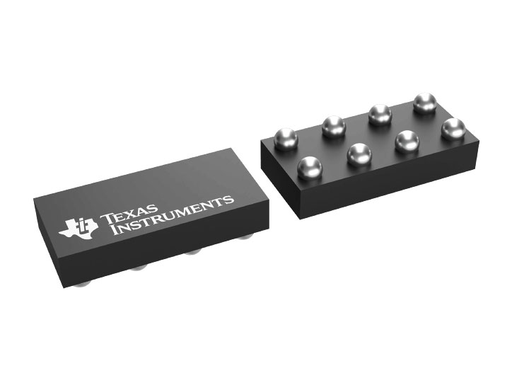
The image is for illustrative purposes only; please refer to the product data sheet for precise specifications.
GET QUOTE NOW!
| Part Number | SN74LVC3G14YZPR |
|---|---|
| Manufacturer |
 Texas Instruments Texas Instruments
|
| Description | The SN74LVC3G14YZPR is a high-speed, low-power triple Schmitt-trigger inverter from Texas Instruments. Designed for digital signal conditioning, waveform shaping, logic inversion, and noise-sensitive switching applications, the device integrates three independent inverting logic gates with Schmitt-trigger inputs in an ultra-compact NanoFree chip-scale package. The SN74LVC3G14 belongs to the 74LVC low-voltage CMOS logic family and operates over a wide supply voltage range of 1.65V to 5.5V. This flexibility allows the device to be integrated into 1.8V, 2.5V, 3.3V, and 5V digital logic systems without requiring different inverter families. Each of the three independent channels implements the Boolean inversion function Y = NOT A. When the input voltage exceeds the positive-going Schmitt-trigger threshold, the corresponding output switches LOW. When the input voltage falls below the negative-going threshold, the output switches HIGH. The integrated Schmitt-trigger input architecture provides hysteresis between the positive-going and negative-going switching thresholds. This hysteresis improves noise immunity and helps prevent unwanted output transitions when input signals contain electrical noise, slow edges, or small voltage fluctuations near the switching threshold. Unlike conventional CMOS inverters, which may produce unstable switching behavior when driven by slowly changing signals, the SN74LVC3G14 is particularly effective for slow-input signal conditioning. The Schmitt-trigger architecture converts gradually changing input voltages into clean digital output transitions. The device supports input voltages up to 5.5V, allowing its inputs to interface with higher-voltage logic signals even when the supply voltage is lower. This feature is particularly useful in mixed-voltage digital systems where 5V signals must be received by logic operating from a 3.3V supply. The SN74LVC3G14 provides excellent switching performance, with a maximum propagation delay of 5.4ns at VCC = 3.3V under the specified test conditions. This fast response makes the device suitable for high-speed digital signal processing, pulse shaping, clock conditioning, and general-purpose logic inversion. The device provides a strong push-pull CMOS output stage with output drive capability of approximately ±24mA at 3.3V under the specified operating conditions. This allows the inverter outputs to drive digital logic inputs, moderate capacitive loads, and other compatible circuitry without requiring an additional buffer in many applications. Low power consumption is another important characteristic of the SN74LVC3G14. The device has a maximum static supply current of only 10µA under specified conditions, making it suitable for battery-powered equipment, portable electronics, embedded controllers, and other applications where minimizing standby power is important. The SN74LVC3G14 includes an integrated Ioff partial-power-down protection feature. When the device is powered down, the Ioff circuitry disables the outputs and helps prevent damaging current backflow through the device. This functionality supports live insertion, partial-power-down systems, and mixed-power-domain applications. The device is particularly useful for mechanical switch debouncing. By combining a Schmitt-trigger inverter with a suitable resistor-capacitor network, designers can suppress unwanted switching transitions caused by mechanical contact bounce and produce a stable digital signal for a microcontroller or other logic device. Another common application is waveform shaping. Slowly changing analog-like signals, RC timing waveforms, and noisy digital inputs can be converted into well-defined CMOS logic levels, improving downstream switching reliability. The Schmitt-trigger architecture also supports the implementation of simple RC relaxation oscillator circuits. By combining an inverter with external resistors and capacitors, designers can generate periodic digital waveforms for timing, blinking indicators, and other nonprecision oscillator applications. The three independent inverter channels can be used separately for different functions within the same circuit. For example, one channel can condition a sensor signal, another can debounce a mechanical switch, and the third can invert a digital control signal. This integration reduces component count and simplifies PCB layout. The device provides robust electrical performance, including latch-up immunity exceeding 100mA according to JESD 78 Class II requirements. Its ESD protection ratings include 2000V Human Body Model, 200V Machine Model, and 1000V Charged Device Model under the applicable test standards. The SN74LVC3G14YZPR is specified for an operating temperature range of -40°C to +125°C. This extended temperature capability supports its use in industrial control equipment, embedded electronics, instrumentation, communication systems, and other applications requiring reliable operation across a wide temperature range. The SN74LVC3G14YZPR is supplied in an ultra-compact 8-ball DSBGA package, identified by Texas Instruments package code YZP. The package uses TI's NanoFree technology, in which the semiconductor die itself forms the basis of the finished chip-scale package. The YZP package occupies approximately 2.81mm2 of PCB area, providing three independent Schmitt-trigger inverter channels in a very small footprint. This makes the device particularly suitable for space-constrained electronics, miniature embedded systems, portable equipment, and densely populated circuit boards. The DSBGA package uses SnAgCu lead-free solder balls and is compatible with automated surface-mount assembly. Proper PCB land-pattern design, solder paste application, placement accuracy, and reflow processing should follow the manufacturer's chip-scale package assembly recommendations. The YZPR ordering designation identifies the NanoFree DSBGA package supplied in tape-and-reel packaging. The standard manufacturer package quantity is 3000 devices per reel, making the component suitable for high-volume automated electronics manufacturing. The SN74LVC3G14YZPR is RoHS and REACH compliant and has a moisture sensitivity classification of MSL 1 with a maximum specified peak reflow temperature of 260°C. The combination of three independent Schmitt-trigger inverters, 1.65V to 5.5V supply operation, 5.5V-tolerant inputs, 5.4ns maximum propagation delay at 3.3V, ±24mA output drive, 10µA maximum static supply current, Ioff protection, -40°C to +125°C operation, and ultra-compact 8-ball NanoFree packaging makes the SN74LVC3G14YZPR an excellent choice for reliable and space-efficient digital signal conditioning. The SN74LVC3G14YZPR is widely used in digital signal conditioning, logic inversion, waveform shaping, mechanical switch debouncing, sensor interfaces, clock signal conditioning, pulse generation, RC oscillator circuits, microcontroller interfaces, industrial control electronics, portable devices, battery-powered equipment, communication systems, instrumentation, embedded controllers, consumer electronics, and general-purpose CMOS logic applications. |
| Product Group | Logic IC |
| MOQ | 3000 pcs |
| SPQ | 3000 pcs |
| Figure/Case | DSBGA-8 |
| Package | T&R Pack |
 PDF Datasheet PDF Datasheet | |
| Ship From | Hong Kong |
| Shipment Way | DHL / Fedex / TNT / UPS / Others |
| Delivery Term | Ex-Works |
| Send RFQ | sales@signalhk.com |
Request quotation for
SN74LVC3G14YZPR
SN74LVC3G14YZPR