Driving LEDs and 7-Segment Displays with Arduino
Overview
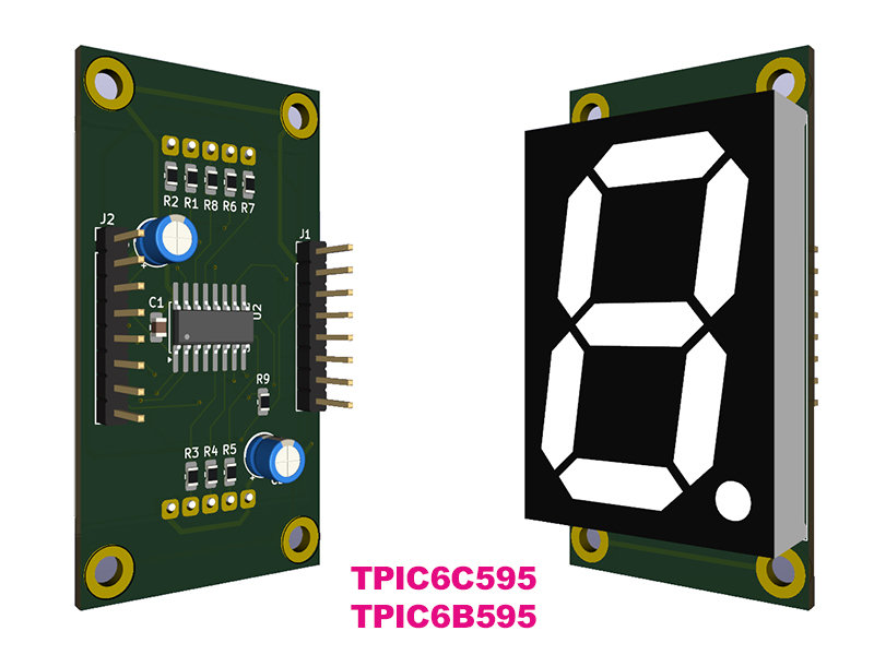
TPIC6C595 and TPIC6B595 are 8-bit shift register + latch driver ICs. They operate exactly the same way; the only difference is their current handling capability.
Summary: TPIC6B595 can drive higher current than TPIC6C595.
How It Works
- Data is sent through the SERIAL-IN pin
- Each clock pulse (SRCK) shifts the data
- After 8 bits, data is latched using RCK
- Outputs are enabled using OE
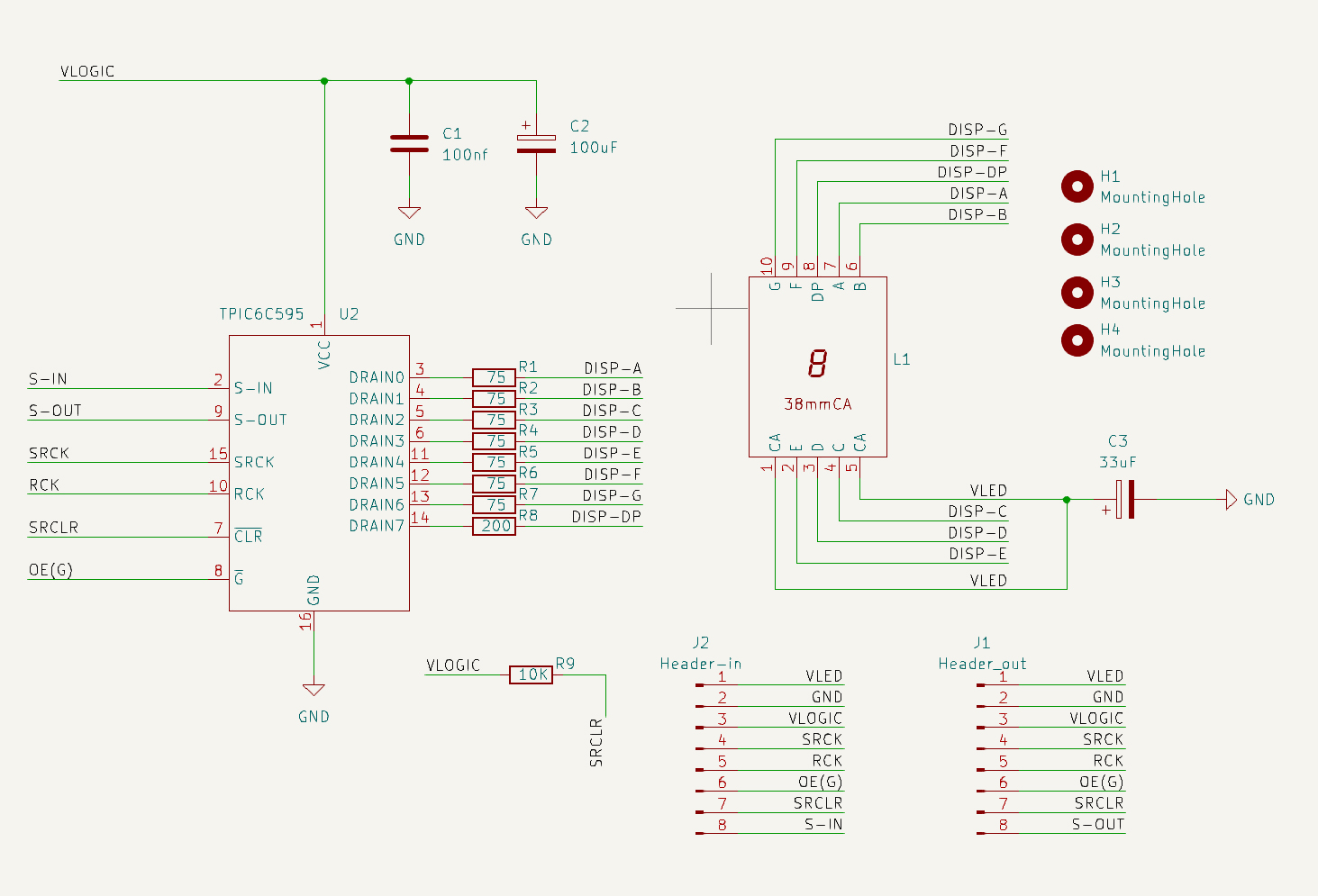
Pin Description
| Pin | Function | Description |
|---|---|---|
| VLED | Load Supply | Power for LEDs or external load |
| GND | Ground | Common reference |
| VLOGIC | Logic Supply | Typically 5V (same as MCU) |
| SERIAL-IN | Data Input | Serial data is fed here |
| SRCK | Shift Clock | Each pulse shifts one bit |
| RCK | Latch Clock | Transfers data to outputs |
| OE (G) | Output Enable | LOW = active, can be used for PWM |
| SRCLR | Clear | LOW clears the shift register |
Data Transfer Sequence
| Step | Action |
|---|---|
| 1 | Write bit to SERIAL-IN |
| 2 | Pulse SRCK (clock) |
| 3 | Repeat until 8 bits are loaded |
| 4 | Pulse RCK to latch data |
| 5 | Set OE LOW to enable outputs |
Output Structure
These ICs are low-side (sink) drivers — they do NOT source current!
- Use common anode displays
- LED positive goes to VLED
TPIC6C595 vs TPIC6B595
| Feature | TPIC6C595 | TPIC6B595 |
|---|---|---|
| Max Current (per channel) | ~100 mA | ~150 mA |
| Typical Use | LEDs | Relays / Motors |
| Logic | Same | |
PWM Brightness Control
The OE pin can be driven with PWM to control brightness:
| PWM Value | Result |
|---|---|
| 0 | Fully ON |
| 255 | OFF |
7-Segment Bit Mapping
| Digit | Binary |
|---|---|
| 0 | 00111111 |
| 1 | 00000110 |
| 2 | 01011011 |
| 3 | 01001111 |
| 4 | 01100110 |
| 5 | 01101101 |
| 6 | 01111101 |
| 7 | 00000111 |
| 8 | 01111111 |
| 9 | 01101111 |
TPIC6x595 Example Application Schematics PDF
- Both ICs work exactly the same
- The only difference is current capacity
- They are low-side (sink) drivers
- PWM can be used for brightness control
Example Code for Arduino for Test
// TPIC6C595 / TPIC6B595 Single Digit 7-Segment Test Code

// Arduino Nano connection:

// VLED      -> External LED/display supply

// GND       -> Arduino GND and external supply GND

// VLOGIC    -> Arduino 5V

// SRCK      -> Arduino D11

// RCK       -> Arduino D10

// OE(G)     -> Arduino D3 PWM

// SRCLR     -> Arduino D9

// SERIAL-IN -> Arduino D8


const int SER_PIN   = 8;   // Serial data input

const int SRCK_PIN  = 11;  // Shift register clock

const int RCK_PIN   = 10;  // Storage/latch register clock

const int OE_PIN    = 3;   // Output Enable, active LOW, PWM capable

const int SRCLR_PIN = 9;   // Shift register clear, active LOW


// Segment bit order: DP G F E D C B A

// These values assume a common-anode 7-segment display.

// Logic 1 turns the corresponding TPIC output ON, sinking current to GND.

byte digits[10] = {

  B00111111, // 0

  B00000110, // 1

  B01011011, // 2

  B01001111, // 3

  B01100110, // 4

  B01101101, // 5

  B01111101, // 6

  B00000111, // 7

  B01111111, // 8

  B01101111  // 9

};


void setup() {

  pinMode(SER_PIN, OUTPUT);

  pinMode(SRCK_PIN, OUTPUT);

  pinMode(RCK_PIN, OUTPUT);

  pinMode(OE_PIN, OUTPUT);

  pinMode(SRCLR_PIN, OUTPUT);


  digitalWrite(SRCLR_PIN, HIGH); // Enable the shift register

  analogWrite(OE_PIN, 255);      // Outputs OFF at startup

}


void sendToTPIC(byte data) {

  digitalWrite(RCK_PIN, LOW);

  shiftOut(SER_PIN, SRCK_PIN, MSBFIRST, data);

  digitalWrite(RCK_PIN, HIGH);

}


// OE(G) is active LOW:

// PWM 0   = fully ON

// PWM 255 = OFF

void fadeDigit(byte digitData) {

  sendToTPIC(digitData);


  // Fade in

  for (int pwm = 255; pwm >= 0; pwm--) {

    analogWrite(OE_PIN, pwm);

    delay(2);

  }


  delay(500);


  // Fade out

  for (int pwm = 0; pwm <= 254; pwm++) {

    analogWrite(OE_PIN, pwm);

    delay(2);

  }


  delay(500);

}


void loop() {

  for (int i = 0; i <= 9; i++) {

    fadeDigit(digits[i]);

  }

}