Introduction
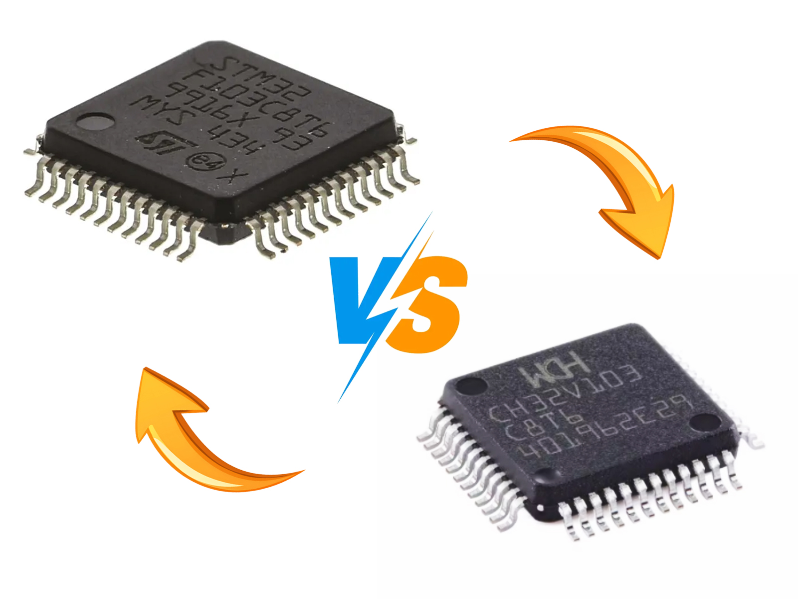
The STM32F103C8T6 from STMicroelectronics and the CH32V103C8T6 from WCH (Nanjing Qinheng Microelectronics) are two 32-bit microcontrollers designed for embedded control, industrial automation, communication interfaces, motor control, and general-purpose electronics.
Although both microcontrollers feature 64 KB of Flash memory, 20 KB of SRAM, 37 GPIO pins, and an LQFP-48 package, they have fundamentally different processor architectures.
The STM32F103C8T6 is based on the Arm Cortex-M3 architecture, while the CH32V103C8T6 uses WCH's QingKe RISC-V3A processor implementing the RV32IMAC instruction set.
The CH32V103C8T6 offers a higher maximum clock frequency, a wider operating voltage range, USB host capability, capacitive touch sensing, and potentially lower hardware costs. The STM32F103C8T6, on the other hand, provides two independent ADC modules, an integrated CAN controller, extensive development tools, and a mature software ecosystem.
This article examines their technical specifications, electrical characteristics, processing capabilities, peripheral interfaces, development environments, compatibility, and practical advantages.
1. Complete Technical Specifications Comparison
The following comparison applies specifically to the 48-pin C8T6 versions, not the higher-pin-count devices in either product family.
| Features | STM32F103C8T6 | CH32V103C8T6 |
|---|---|---|
| General Specifications | ||
| Manufacturer | STMicroelectronics | WCH (Nanjing Qinheng Microelectronics) |
| Microcontroller Family | STM32F1 | CH32V1 |
| Processor Architecture | Arm Cortex-M3 | QingKe RISC-V3A |
| Instruction Set | Arm Thumb-2 | RISC-V RV32IMAC |
| CPU Architecture Width | 32-bit | 32-bit |
| Maximum CPU Frequency | 72 MHz | 80 MHz |
| Typical USB-Compatible CPU Clock | 72 MHz | 48 or 72 MHz PLL configuration |
| Hardware Multiplication | Yes | Yes |
| Hardware Division | Yes | Yes |
| Hardware FPU | No | No |
| Interrupt Controller | NVIC | PFIC |
| Memory Specifications | ||
| Program Flash Memory | 64 KB | 64 KB |
| SRAM | 20 KB | 20 KB |
| Flash Endurance | 10,000 cycles minimum | 10,000 cycles minimum |
| EEPROM | No dedicated EEPROM | No dedicated EEPROM |
| Additional User Configuration Storage | Option bytes and backup registers | 128 bytes of user-defined nonvolatile configuration storage |
| System Bootloader | Factory-programmed ROM bootloader | Factory-programmed ROM bootloader |
| Electrical and Physical Specifications | ||
| Operating Voltage (VDD) | 2.0–3.6 V | 2.7–5.5 V |
| Nominal 3.3 V Operation | Yes | Yes |
| Nominal 5 V Operation | No | Yes |
| Operating Temperature | −40°C to +85°C | −40°C to +85°C |
| Package | LQFP-48 | LQFP-48 |
| Package Body Dimensions | 7 × 7 mm | 7 × 7 mm |
| Pin Pitch | 0.5 mm | 0.5 mm |
| Available GPIO Pins | 37 | 37 |
| GPIO Voltage Characteristics | Many digital pins are 5 V tolerant; analog pins are exceptions | GPIO operates with the device supply; pin limits depend on operating conditions |
| External Interrupt Lines | 16 GPIO EXTI lines | 16 GPIO EXTI lines |
| Analog Peripherals | ||
| ADC Resolution | 12-bit | 12-bit |
| Number of ADC Modules | 2 | 1 |
| External ADC Input Channels | 10, shared by the ADC modules | 10 |
| Maximum ADC Sampling Rate | Approximately 1 MSPS per ADC | Approximately 1 MSPS |
| Internal Temperature Sensor | Yes | Yes |
| Capacitive Touch Sensing (TouchKey) | No dedicated TouchKey module | Yes, up to 10 external channels on this package |
| DAC Modules | None | None |
| Analog Comparators | No general-purpose comparator | No general-purpose comparator |
| Timers and Control Peripherals | ||
| General-Purpose 16-bit Timers | 3 | 3 |
| Advanced-Control 16-bit Timers | 1 | 1 |
| PWM Generation | Yes | Yes |
| Complementary PWM with Dead Time | Yes | Yes |
| Quadrature Encoder Interface | Yes | Yes |
| Independent Watchdog (IWDG) | 1 | 1 |
| Window Watchdog (WWDG) | 1 | 1 |
| System Timer (SysTick) | 24-bit downcounter | 64-bit upcounter |
| DMA Controller | 7 channels | 7 channels |
| Communication Interfaces | ||
| USART Interfaces | 3 | 3 |
| Maximum USART1 Rate | 4.5 Mbit/s | 4.5 Mbit/s |
| SPI Interfaces | 2 | 2 |
| Maximum Stated SPI Data Rate | 18 Mbit/s | 36 Mbit/s |
| I²C Interfaces | 2 | 2 |
| I²C / SMBus Support | Yes | Yes |
| Integrated CAN Controller | 1 × CAN 2.0B | None |
| CAN FD | No | No |
| USB Controller | USB 2.0 Full-Speed device | USB 2.0 host/device |
| USB Device Support | Yes | Yes |
| USB Host Support | No | Yes |
| USB Full-Speed Signaling | 12 Mbit/s | 12 Mbit/s |
| USB Low-Speed Host Support | No host functionality | Yes |
| Clock, RTC and Power Management | ||
| RTC | Yes | Yes |
| Backup Battery Input (VBAT) | Yes | Yes |
| Internal High-Speed Oscillator | 8 MHz | 8 MHz |
| Internal Low-Speed Oscillator | Approximately 40 kHz | Approximately 40 kHz |
| External High-Speed Crystal | 4–16 MHz | 4–16 MHz |
| External RTC Crystal | 32.768 kHz | 32.768 kHz |
| Clock Security System | Yes | Yes |
| Brownout / Power Monitoring | POR/PDR and PVD | POR/PDR and PVD |
| CRC Hardware Calculation | Yes | Yes |
| Unique Device Identifier | 96-bit | 96-bit |
| Low-Power Modes | Sleep, Stop, Standby | Sleep, Stop, Standby |
| Software and Development | ||
| Primary Debugging Interface | Arm SWD / JTAG | WCH two-wire SDI |
| Common Development Probe | ST-LINK | WCH-Link / WCH-LinkE |
| Primary Official IDE | STM32CubeIDE | MounRiver Studio |
| Primary Firmware Libraries | STM32 HAL, LL, legacy SPL | WCH peripheral libraries and EVT examples |
| Compiler Architecture | Arm embedded GCC / Arm toolchains | RISC-V GCC toolchain |
| STM32CubeMX Support | Yes | No native device support |
| Direct Firmware Binary Compatibility | Arm executable | Not compatible with Arm executable |
| Pin Compatibility | STM32F103 reference layout | Same primary LQFP-48 pin positions; functional differences exist |
| Typical Component Cost Positioning | Generally higher | Often lower, depending on supplier and quantity |
Important specification notes: The CH32V103's maximum 80 MHz CPU rating should not be confused with its USB operating configuration, which requires a 48 MHz USB clock derived from a 48 or 72 MHz PLL. The CH32V103 family supports more ADC and TouchKey channels in larger packages, but the C8T6 version exposes 10 external channels. Both devices have no hardware floating-point unit.
2. Processor Architecture and Performance
STM32F103C8T6: Arm Cortex-M3
The STM32F103C8T6 integrates an Arm Cortex-M3 processor operating at a maximum frequency of 72 MHz.
The Cortex-M3 is a widely adopted embedded architecture, offering efficient interrupt processing, 32-bit arithmetic, deterministic peripheral control, and extensive compiler support.
Its main architectural advantages include the Thumb-2 instruction set, hardware multiplication and division, Nested Vectored Interrupt Controller (NVIC), and automatic interrupt context handling.
ST specifies a performance rating of 1.25 DMIPS/MHz under its stated benchmark conditions, corresponding to a nominal 90 DMIPS at 72 MHz. This figure should not be treated as a direct benchmark comparison with the CH32V103.
CH32V103C8T6: QingKe RISC-V3A
The CH32V103C8T6 uses WCH's QingKe RISC-V3A processor, implementing the RV32IMAC instruction set.
This instruction set includes integer operations, hardware multiplication and division, atomic instructions, and compressed instruction encoding.
The processor incorporates instruction prefetching, a short pipeline, branch prediction, and WCH's Programmable Fast Interrupt Controller (PFIC).
The maximum specified operating frequency is 80 MHz, approximately 11.1% higher than the STM32F103's 72 MHz limit.
However, a higher clock frequency does not automatically translate into 11.1% higher application performance.
Execution efficiency depends on the instruction set, compiler optimization, Flash access latency, memory behavior, interrupt overhead, and application workload.
For applications involving PWM control, SPI communication, GPIO manipulation, and embedded state machines, both processors provide adequate processing capability.
Architecture Analysis
The STM32F103 is particularly attractive when the project already depends on Arm libraries, CMSIS, ST middleware, or an existing STM32 firmware codebase.
The CH32V103 becomes attractive for new designs where the firmware can be built specifically for RISC-V and where reduced component cost or additional peripheral functions are important.
The RISC-V instruction set is an open standard, but the QingKe processor implementation and certain vendor-specific features remain WCH-specific.
3. Memory Architecture
Both devices provide 64 KB of internal Flash memory and 20 KB of SRAM.
This capacity is generally suitable for industrial controllers, sensor acquisition systems, LED drivers, motor control boards, communication gateways, and compact USB peripherals.
However, firmware size can grow significantly when USB class stacks, large lookup tables, or graphical libraries are included.
The STM32F103C8T6 also belongs to an established product family with devices offering higher Flash capacities, although upgrading to another part requires checking the exact package and peripheral compatibility.
The CH32V103C8T6 includes a factory bootloader area of approximately 3.75 KB and a separate 128-byte user-defined nonvolatile configuration area.
For designs frequently updating parameters, dedicated external EEPROM or wear-leveled Flash storage may still be necessary.
Both devices specify a minimum Flash endurance of 10,000 erase/program cycles. Actual data retention and endurance depend on the manufacturer's specified operating and testing conditions.
4. Electrical Characteristics and Power Supply
One of the most significant differences is the operating voltage range.
The STM32F103C8T6 operates from 2.0 V to 3.6 V and is normally powered using a regulated 3.3 V supply.
The CH32V103C8T6 supports 2.7 V to 5.5 V, allowing it to operate from either a 3.3 V supply or a nominal 5 V supply.
This can simplify designs using 5 V-powered sensors, logic interfaces, or other external devices.
However, operating at 5 V does not automatically guarantee that every connected device is electrically compatible. The input-high thresholds, analog input limits, USB interface requirements, and current ratings must still be verified.
Additionally, WCH specifies separate operating limits for the analog and USB functions. For example, the CH32V103 ADC is specified with VDDA starting at 3.0 V, even though the general MCU operating voltage extends down to 2.7 V.
Published Power-Consumption Figures
| Features | STM32F103C8T6 | CH32V103C8T6 |
|---|---|---|
| Run Mode at 72 MHz, Peripherals Disabled | 27 mA typical | 8.88 mA typical |
| Run Mode at 72 MHz, Peripherals Enabled | 36 mA typical | 13.56 mA typical |
| Stop Mode, Regulator in Low-Power Mode | 14 µA typical at 3.3 V | 1.6 µA typical |
| Standby Mode, Watchdog and RTC Disabled | 2.0 µA typical at 3.3 V | 1.6 µA typical |
| VBAT Backup Current, RTC Enabled | 1.4 µA typical at 3.3 V | 2.4 µA typical |
Values are reproduced from the manufacturers' respective electrical-characteristics tables. Test configurations are not identical, and these figures are not a controlled, side-by-side benchmark.
The CH32V103 shows significantly lower published Run-mode current figures at 72 MHz under its manufacturer's test conditions. It also has a low reported Stop-mode current when the regulator is configured for low-power operation.
For battery-powered products, the final choice should depend on measured current with the complete firmware and all required peripherals operating.
5. ADC and Analog Capabilities
The STM32F103C8T6 includes two 12-bit ADC units, whereas the CH32V103C8T6 includes one.
Both devices expose 10 external analog input channels in their 48-pin variants and offer a maximum conversion rate of approximately one million samples per second per ADC.
The STM32's dual-ADC architecture can provide a useful advantage in applications requiring synchronized or simultaneous sampling.
This is particularly relevant for motor-control systems, current measurement, dual-sensor monitoring, and closed-loop control applications.
The CH32V103 compensates with its built-in capacitive touch-key sensing function.
Capacitive touch detection can eliminate external touch-controller ICs in products such as control panels, appliances, lighting interfaces, and compact human-machine interfaces.
Neither MCU contains a general-purpose DAC. Applications requiring true analog output need an external DAC or a filtered PWM signal.
The ADC voltage range follows the analog supply/reference arrangement, so a 5 V-powered CH32V103 analog system is not automatically measurement-compatible with a 3.3 V STM32 design.
6. Timers, PWM and Motor Control
Both microcontrollers integrate three general-purpose 16-bit timers and one advanced-control 16-bit timer.
These peripherals support input capture, output comparison, PWM generation, pulse counting, and quadrature encoder input modes.
The advanced-control timers support complementary PWM outputs, programmable dead time, and emergency shutdown functions.
These capabilities make both MCUs suitable for:
- DC motor control
- Stepper motor pulse generation
- LED dimming
- Servo applications
- Rotary encoder acquisition
- Small industrial control systems
For example, both MCUs can be used to drive a constant-current LED matrix driver through SPI while using an internal timer to regulate the display refresh rate.
The CH32V103's 80 MHz clock capability provides extra timer resolution for certain configurations. However, actual usable timing resolution depends on the timer clock source and prescaler arrangement.
The STM32F103 also benefits from mature motor-control examples and libraries.
7. Communication Interfaces
Both microcontrollers provide three USART interfaces, two SPI interfaces, and two I²C interfaces.
The CH32V103's SPI controller supports a manufacturer-stated maximum clock rate of 36 MHz, compared with the STM32F103's stated 18 Mbit/s SPI capability.
This provides a potential benefit in applications using SPI displays, external Flash devices, ADC interfaces, and high-speed shift-register or LED-driver chains.
The actual achievable transfer rate depends on clock configuration, signal integrity, PCB routing, and external device limits.
CAN Communication
The STM32F103C8T6 contains a CAN 2.0B controller, suitable for industrial and embedded CAN systems when combined with an external CAN transceiver.
The CH32V103C8T6 does not include an integrated CAN controller.
This difference is critical for applications requiring CAN communication because replacing the STM32 with the CH32V103 would require an external CAN controller or a different MCU selection.
There is also an important STM32F103 limitation: its USB and CAN peripherals share dedicated packet SRAM and cannot operate concurrently. They can exist in the same firmware but must not be active simultaneously.
USB Communication
The STM32F103C8T6 provides USB 2.0 Full-Speed device operation. It can act as a USB peripheral connected to a PC or another host.
The CH32V103C8T6 includes a USB controller supporting both host and device functionality.
This enables potential applications involving USB keyboards, mice, removable USB devices, or custom USB peripherals, provided suitable firmware and the required host-side power circuitry are implemented.
The CH32V103's USB controller requires a 48 MHz USB clock derived from a 48 MHz or 72 MHz PLL configuration. Consequently, its 80 MHz maximum core frequency should not be assumed available during ordinary USB operation.
For the STM32F103, USB device designs also require attention to the D+ pull-up arrangement and the correct 48 MHz USB clock.
8. Pinout and Hardware Compatibility
Both microcontrollers use a 48-pin LQFP package with a 7 × 7 mm body and 0.5 mm pin pitch.
The primary physical pin arrangements match, including the main supply pins, oscillator connections, reset pin, boot-selection pins, and GPIO port numbering.
Common connections include:
| Features | STM32F103C8T6 | CH32V103C8T6 |
|---|---|---|
| Pin 1 | VBAT | VBAT |
| Pin 7 | NRST | NRST |
| Pin 8 | VSSA | VSSA |
| Pin 9 | VDDA | VDDA |
| Pin 10 | PA0 | PA0 |
| Pin 30 | PA9 / USART1 TX | PA9 / USART1 TX |
| Pin 31 | PA10 / USART1 RX | PA10 / USART1 RX |
| Pin 32 | PA11 / USB D− | PA11 / USB D− |
| Pin 33 | PA12 / USB D+ | PA12 / USB D+ |
| Pin 34 | PA13 / Debug Data | PA13 / Debug Data |
| Pin 35 | VSS | VSS |
| Pin 36 | VDD | VDD |
| Pin 37 | PA14 / Debug Clock | PA14 / Debug Clock |
| Pin 44 | BOOT0 | BOOT0 |
| Pin 48 | VDD | VDD |
This matching pin arrangement makes the CH32V103C8T6 a potential PCB-level alternative for certain STM32F103C8T6 designs.
However, pin-compatible does not mean electrically, functionally, or firmware-compatible.
An existing PCB must still be checked for its power supply, USB components, alternate-function mapping, analog circuitry, programming interface, boot configuration, and peripheral dependencies.
9. Firmware Development and Debugging
STM32F103C8T6 Software Environment
STMicroelectronics provides STM32CubeIDE, STM32CubeMX, STM32 HAL/LL drivers, and extensive technical documentation.
Developers can also use Keil MDK, IAR Embedded Workbench, GCC-based toolchains, and various third-party embedded frameworks.
The Arm Cortex-M3 architecture benefits from broad support for CMSIS, FreeRTOS, middleware, and debugging tools.
Programming and debugging are typically performed through ST-LINK using SWD or JTAG.
CH32V103C8T6 Software Environment
WCH provides MounRiver Studio, its official development environment for CH32 microcontrollers.
WCH also supplies peripheral driver libraries, example projects, and evaluation resources.
The CH32V103 is programmed and debugged using WCH-compatible equipment such as WCH-Link or WCH-LinkE.
Although the debug pins are named SWDIO and SWCLK and occupy positions similar to those on the STM32F103, the RISC-V debugging implementation is different. A normal ST-LINK setup should not be assumed to work with the CH32V103.
The CH32V103 can be programmed through its manufacturer-supported system bootloader, including USART1 and USB interfaces.
By contrast, the STM32F103C8's factory ROM bootloader supports USART programming but does not provide a factory USB DFU bootloader.
Firmware Portability
STM32F103 firmware binaries cannot execute directly on a CH32V103.
The microcontrollers have different instruction sets, startup sequences, interrupt controllers, core registers, linker configurations, and debugging implementations.
A migration generally requires:
- Recompiling the application for RISC-V.
- Replacing STM32-specific driver calls.
- Adapting interrupts and startup code.
- Updating linker scripts and memory configuration.
- Validating peripheral initialization.
- Testing communication interfaces and timing behavior.
- Verifying the complete application on the target hardware.
Applications based on portable C code are easier to migrate than projects containing extensive STM32 register-level programming or Arm assembly.
10. Practical Applications and Selection Analysis
Industrial Automation
Both microcontrollers can handle sensor acquisition, GPIO control, timers, relays, serial communication, and control logic.
The STM32F103 has an advantage when integrated CAN communication is required.
USB Peripherals
Both devices can implement USB device applications.
The CH32V103 is additionally attractive when USB host functionality is required.
LED Matrix Controllers
Both devices have sufficient Flash, RAM, SPI, and timer resources for LED animation and driver control.
The CH32V103's faster SPI specification and published Run-mode current figures may be advantageous for cost-sensitive products.
Motor Control
Both provide advanced PWM timers, dead-time generation, and encoder interfaces.
The STM32F103's two ADC modules may be advantageous for simultaneous analog measurements.
Battery-Operated Controllers
Either device can be considered.
The CH32V103's published low-power figures are competitive, but board-level measurements are needed before drawing a definitive energy-efficiency conclusion.
Capacitive Touch Panels
The CH32V103 has a clear functional advantage because of its dedicated TouchKey peripheral.
Existing STM32 Products
The STM32F103 remains the easier choice when firmware compatibility, existing development infrastructure, testing investment, and maintenance costs outweigh a potential component-price reduction.
11. Advantages and Disadvantages
STM32F103C8T6
Advantages
- Mature Arm development ecosystem.
- Extensive documentation, middleware, and community support.
- Two independent 12-bit ADC modules.
- Integrated CAN 2.0B controller.
- Broad debugger and software-tool support.
- Good choice for maintaining existing STM32-based products.
Disadvantages
- Limited to a maximum 3.6 V supply.
- Maximum CPU clock of 72 MHz.
- USB device functionality only.
- No dedicated capacitive TouchKey peripheral.
- USB and CAN cannot operate simultaneously.
- Often higher acquisition cost than cost-oriented alternatives.
CH32V103C8T6
Advantages
- Up to 80 MHz maximum CPU frequency.
- Wide 2.7–5.5 V operating range.
- USB host and device capability.
- Dedicated capacitive TouchKey functionality.
- Higher manufacturer-stated SPI transfer rate.
- Competitive published power-consumption characteristics.
- Attractive potential cost for volume production.
Disadvantages
- No integrated CAN controller.
- Only one ADC module.
- Not compatible with Arm firmware binaries.
- Requires a RISC-V toolchain and WCH-compatible programming/debugging support.
- Smaller software and middleware ecosystem than STM32.
- USB clock requirements restrict the use of the maximum CPU clock.
- Migration requires firmware modifications and hardware validation.
12. Final Engineering Assessment
The STM32F103C8T6 and CH32V103C8T6 occupy a similar hardware class but serve somewhat different design priorities.
The STM32F103C8T6 is the stronger choice when the application relies on Arm software compatibility, dual ADC sampling, integrated CAN functionality, extensive middleware, or long-established STM32 development practices.
The CH32V103C8T6 is particularly attractive for new, cost-sensitive embedded products that can benefit from 5 V operation, capacitive touch sensing, high-speed SPI, and USB host functionality.
For a new LED controller, motor-control accessory, industrial I/O board, or compact USB peripheral where CAN communication is unnecessary, the CH32V103C8T6 is a technically credible candidate.
However, replacing an STM32F103C8T6 with a CH32V103C8T6 should be treated as a validated hardware substitution combined with a firmware port, not a direct drop-in replacement.
The final selection should consider complete system cost rather than the microcontroller purchase price alone. Firmware development time, debugging tools, hardware qualification, power consumption, peripheral requirements, and long-term component availability can be more important than a small difference in unit cost.